



Co-Packaged Optics
Key devices for realizing future networks
The widespread adoption of services like Generative AI and cloud computing is driving data centers to support higher speeds and greater capacities, resulting in ongoing increases in power consumption. Some estimates suggest that, at the current pace, the power consumption of data centers will account for about 10% of total global power consumption in 2030. Therefore, data center power saving (greening) has become an urgent issue. Photonics-Electronics Convergence technology is expected to be one solution to this challenge. Integrating optoelectronics into electronic devices and replacing electrical wiring with photonic wiring will increase network capacity while reducing latency, and significantly reduce the power consumption of the systems constituting a network.
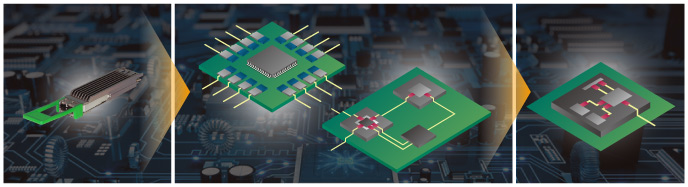
Steps Leading to the Development of Photonics-Electronics Convergence
The convergence of the circuits that handle electrical and optical signals is called photonics-electronics convergence. Several generations of this technology, such as LPO, CPO, and NPO*1, are currently in the research and development stage. The first generation is the “optical module type” with miniaturized optical transceivers (optical engines) mounted near a logic chip, such as an ASIC, to form a module. The next generation is the "high-performance semiconductor package type" which uses chiplets*2.
*1: LPO: linear drive pluggable optics, CPO: co-packaged optics, NPO: near-packaged optics
*2: chiplet: A small bare chip (die) manufactured for a specific function using an optimal process.
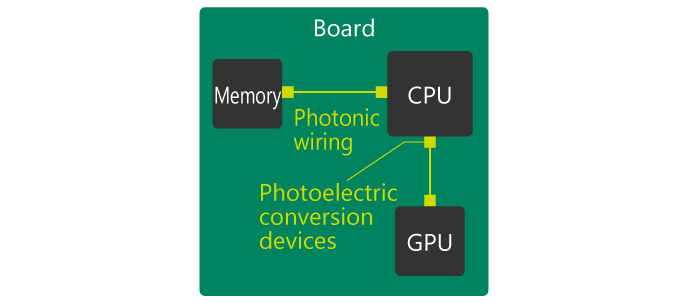
Photonic wiring between chips
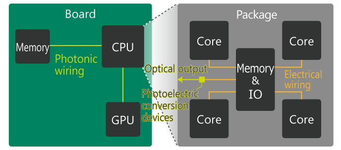
Photonic wiring between cores and memory within a chip
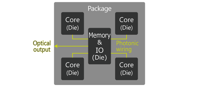
Photonic wiring between dies within a package
Testing Challenges

Photonics-electronics convergence devices exchange both electrical and optical signals. Therefore, to ensure device quality, it is necessary to evaluate multiple aspects, including electrical characteristics, photonic characteristics, and digital signal quality.
Photonic characteristics:
Factors such as insertion loss and reflection (S-parameters) in the photonic wiring, as well as decreased optical output due to heat generation from the light source, can degrade optical transmission performance.
Electrical characteristics:
The transmission/reflection properties (S-parameters) and characteristics of high-frequency circuits can lead to signal degradation.
Digital signal quality:
Eye patterns, jitter, bit error rate, and noise tolerance, all of which are essential measures of digital signal quality in photonics-electronics convergence devices, significantly affect the overall device performance.
The comprehensive evaluation of these characteristics enhances the reliability of photonics-electronics convergence technology.
Test Solutions
Anritsu provides test solutions for evaluating photonics-electronics convergence devices. These solutions can determine the photonic and electrical characteristics, as well as perform digital signal quality testing.
Photonic characteristics:
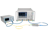
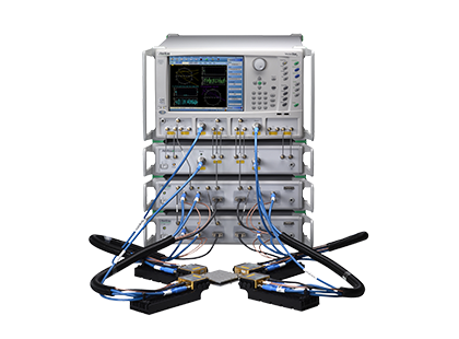
By utilizing Anritsu’s Opto-Electronic Network Analyzer ME7848A, users can evaluate the insertion loss and reflection (S-parameters) in optical wiring. The characteristics of the optical wavelength and output can be clarified using the Optical Spectrum Analyzer MS9740B.
Video:
Anritsu 110 GHz Opto-electronic Network Analysis system (ONA) solution
Electrical characteristics:
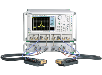
Anritsu’s wideband vector network analyzer ME7838A/D/G series can measure the S-parameters of high-frequency circuits across a wide frequency range up to 220 GHz. Optional features also allow the visualization of eye patterns.
Leaflet:
Digital signal quality:
Anritsu’s Signal Quality Analyzer-R MP1900A is a high-performance, 8-slot modular BERT that enables the evaluation of digital signal jitter, bit error rate, and noise tolerance.
Furthermore, Anritsu’s sampling oscilloscope BERTWave MP2110A is ideal for evaluating photonics-electronics convergence devices from 10G to 1.6T, supporting the measurement of amplitude, jitter, and skew from eye patterns such as PAM4 with a single instrument. By being able to handle up to four channels simultaneously, it contributes to improved production efficiency and reduced manufacturing costs.
By combining these test solutions, manufacturers can ensure the quality of their photonics-electronics convergence devices.
Leaflet:

Resources

Interview (PDF):
Synergy between Nanophotonics and Terahertz with Advanced Electromagnetic Field Analysis
– Interview with Professor Jun Shibayama, Hosei University –
Anritsu interviewed Prof. Jun Shibayama of Hosei University about the development of functional devices in both fields and cutting-edge research, such as the application of optical sensing technology to the terahertz domain.
White paper:
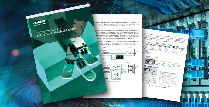
The Pluggable Coherent Revolution: 400ZR and 100ZR Bring Operational Efficiency and Flexibility
This white paper introduces the latest trends in pluggable coherent technology and highlights some use cases utilizing 100ZR, 400ZR, and OpenZR+.







Related Products

Contact Us


Copyright 2026