



Double Data Rate (DDR)
Optimize DDR memory testing
Double Data Rate (DDR) is a technical specification for data transfer at both the clock-signal rise and fall edges and is one standard for RAM used as computer main memory.
The Joint Electron Device Engineering Council (JEDEC) defines three DDR standards:
- Standard DDR for servers and PCs
- Mobile and in-vehicle DDR
- Graphics DDR for high-speed data processing, such as in data centers and AI
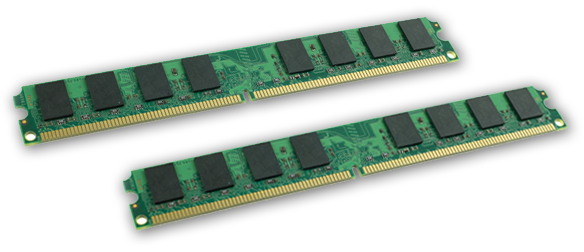
DDR Challenges in R&D
Memory must of course meet the JEDEC specifications and interconnectivity must be assured for devices controlling memory and for systems using RAM. Testing electrical characteristics, such as the clock signal, data-signal voltage changes, rising and falling edge timing, jitter, and others, and communicating the results to designers is a vital step in product development.
DDR Test Solutions
Both transmitter (Tx) and receiver (Rx) tests are used to improve and assure the digital signal quality at the RAM PHY layer.
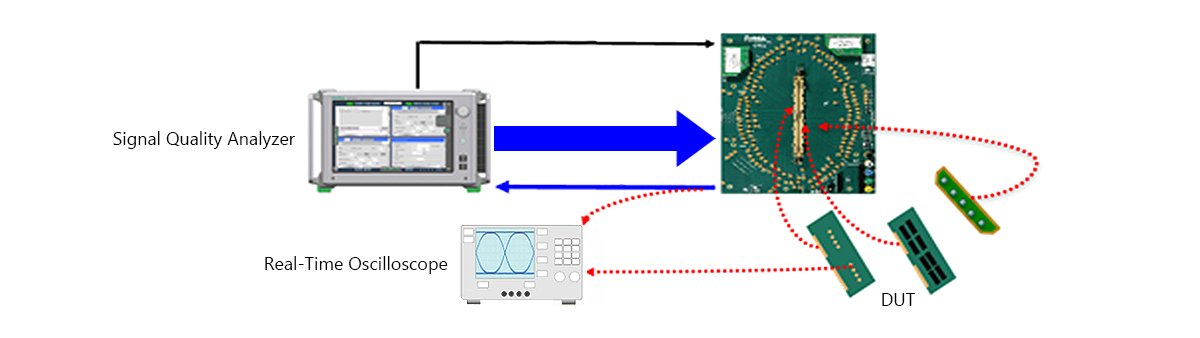
Transmitter and Receiver Tests
The Tx test evaluates the characteristics of the data signal output from the memory using a real-time oscilloscope (RTO) to evaluate the rise/fall times, voltage changes, Eye pattern, jitter, and more, of the reference clock and data-signal output from the USB device. In addition, the phase locked loop (PLL) bandwidth is measured by the RTO using a pulse pattern generator (PPG) as the signal source.
The Rx test uses a PPG and bit error rate (BER) tester to create stress, such as noise and jitter, on the electrical signals to evaluate the RAM jitter tolerance, crosstalk, operation margin, and others.
Resources

See More



Related Products
Contact Us



 Your Privacy Choices
Copyright 2026