



High-Speed Digital Systems
Challenging the digital data transfer limit
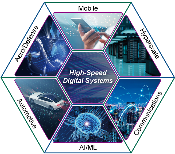
Data traffic is growing rapidly due to the spread of AI in a wide range of industries, high-definition video streaming services, advances in autonomous driving technologies, and many others. Furthermore, AI and disaggregation technologies are being introduced in the network and computing fields. The high-speed digital interfaces, including PCI Express® (PCIe®), USB, DDR, and DisplayPort, are the backbone of these technologies. The interfaces are essential for high-speed digital systems such as computing, server, and storage systems, and the performance continues to evolve daily.
PCI-SIG®, PCIe® and PCI Express® are registered trademarks of PCI-SIG.
Chip
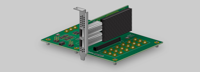
Add-In Card

Photonic wire
Connector
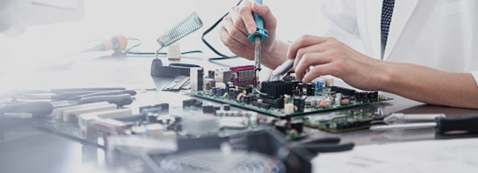
Prototype Debug

Final Prototype Evaluation

Compliance Test
High-Speed Digital System Challenges
Signal degradation due to the characteristics of higher digital signal frequencies and high-frequency loss characteristics of materials used in transmission lines are the main technical challenges facing high-speed digital systems. The impact of jitter*1, crosstalk*2, and degraded Eye characteristics*3 can occasionally cause poor high-speed digital system operation margins.
- *1 Jitter:
- Jitter is variation in timing on the digital-signal time axis.
- Timing is determined by the frequency, pulse width, duty cycle, and the difference in time between the rise and fall edges of the pulse.
- It is caused by various factors, such as noise in the circuit and communications path, and changes in other circuits and external equipment.
- *2 Crosstalk:
- Crosstalk is the phenomenon of signal leakage between adjacent signal wires (buses).
- High crosstalk causes poor operation of high-speed digital systems.
- *3 Eye Characteristics:
- Eye characteristics can be evaluated from eye diagram, which is a graphical display of the [0] and [1] data stream in serial data signals. This is used to evaluate the quality of digital signals.
High-Speed Digital System Test Solutions
These solutions can help resolve challenging issues.




Case Study
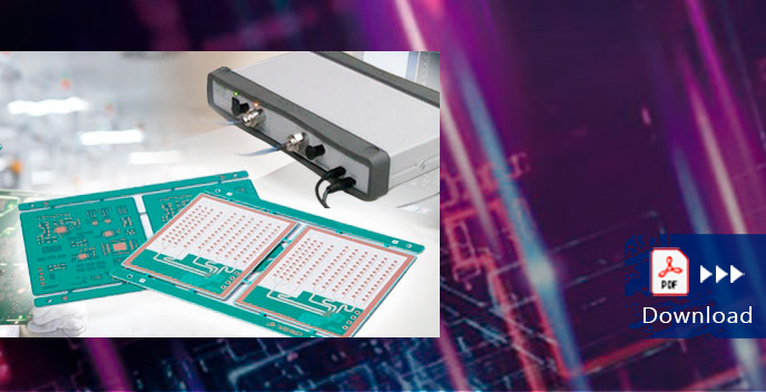
Meiko Electronics Vietnam Co., Ltd.
A global high performance PCB manufacturer completes in factory high frequency PCB evaluation. VNAs drive reliability and proposal strength.
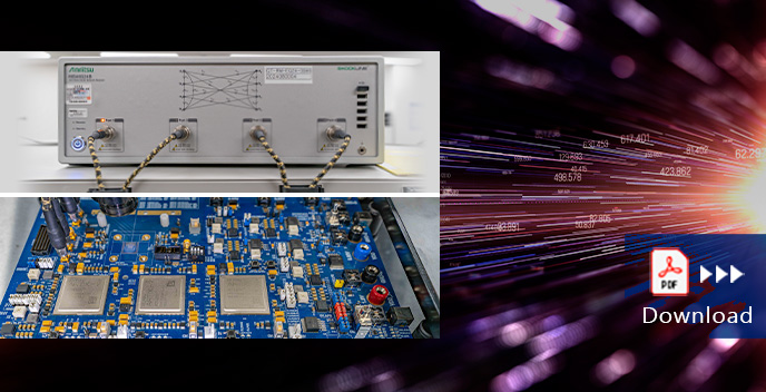
Qualitas Semiconductor Co., Ltd.
A leading company in high-speed interconnect IP development enhanced its verification capabilities and development efficiency by leveraging Anritsu’s vector network analyzer.
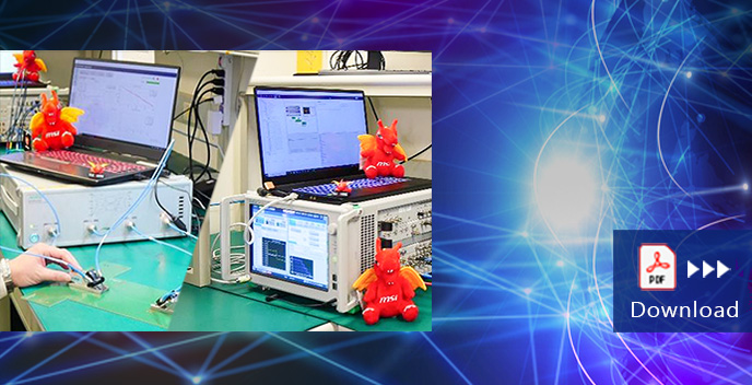
Micro-Star International Co., Ltd.
Overcoming the technical issues hindering high-speed digital transmission in the development of cutting-edge PCs and peripheral devices.
What has been achieved using a BER tester and VNA?
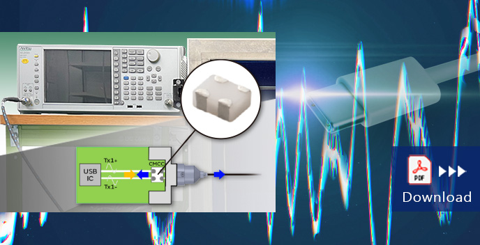
Murata Manufacturing Co., Ltd.
Addressing electromagnetic noise issues in USB 3.2 communication,
while establishing an evaluation environment compliant with RFI testing spec
Resources

Contact Us



 Your Privacy Choices
Copyright 2026