
High-Frequency Device Technologies – Heterojunction Bipolar Transistor –
Transistor High-Frequency Performance Index
Improving the performance of integrated circuits (ICs) in the latest measuring instruments and communication systems requires increasing the operating frequency of the transistors. We have been working on high-performance heterojunction bipolar transistors (HBT) using III-V compound semiconductors.
The HBT high-frequency performance parameters include current gain cut-off frequency (fT) and maximum oscillation frequency (fmax), which can be used to estimate the IC operating frequency. For example, it is generally considered that a high-frequency amplifier IC requires an HBT with an fmax of two to three times the system frequency.
fT, fmax Improvement and Related Parameters
The HBT fT and fmax are defined as follows1):
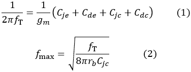
where gm is the transconductance, Cje is the base-to-emitter junction capacitance, Cde is the base-to-emitter diffusion capacitance, Cjc is the base-to-collector capacitance, Cdc is the base-to-collector diffusion capacitance, and rb is the base resistance.
Figure 1 shows the HBT structure and the pi-equivalent circuit. Narrowing the emitter width We, reduces the junction capacitance Cje, Cjc as well as the parasitic resistance rb, thus improving fT and fmax.
Therefore, device microfabrication technology and proper design of the semiconductor layer structure are key to improving HBT performance. Semiconductor design techniques are also required, such as reducing parasitic resistive components by making the base layer dense and thin, and reducing electron travel time by optimizing the collector layer structure.
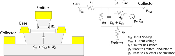
Figure 1 HBT Structure (left) and Pi-Equivalent Circuit (right)
HBT High-Speed Trends
We have developed HBTs using gallium arsenide (GaAs) and indium phosphide (InP) for the compound semiconductor materials. Our first-generation (Gen1) InP-base HBTs with an fT of 200 GHz are faster than GaAs HBTs and was developed realizing ICs for our measuring instruments. A second generation (Gen2) HBT with an fT of 300 GHz has been newly developed with life tests confirming reliability. The Gen2 HBT emitter width is reduced to 0.5 μm (half that of Gen1) and the base resistance is also reduced by increasing the base-layer doping concentration. Figure 2 shows an example of Gen2 HBT high-frequency evaluation results.
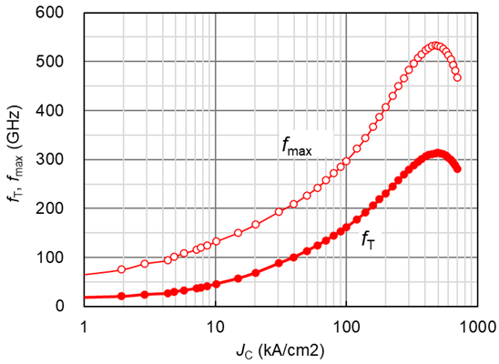
Figure 2 Gen2 HBT High-Frequency Evaluation Example
Figure 3 shows the theoretical IC fT, fmax and operating speed2) for each IC generation using Gen1, Gen2 HBTs and digital IC. GaAs-based HBTs are expected to achieve IC operating speeds of 40 Gbit/s, while ICs using Gen1 HBTs reach 100 Gbit/s, and ICs using the newly developed Gen2 HBTs reach 160 Gbit/s.
In future, we plan to develop next-generation faster HBTs to reach higher IC frequency ranges.
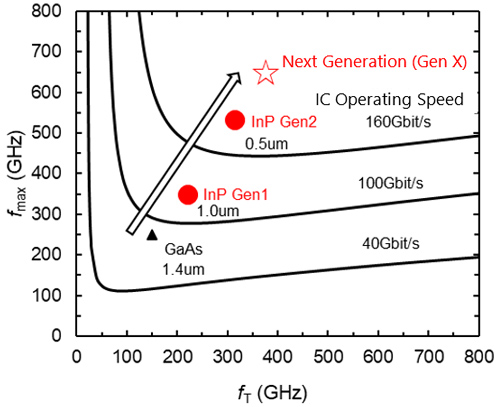
Figure 3 High-Frequency Characteristic and Theoretical IC Operation Speed for Each HBT Generation
References
1) https://www.ieice-hbkb.org/portal/doc_600.html (in Japanese)
2) E. Sano, Y. Matsuoka, T. Ishibashi, IEICE Trans. Electron., vol. E78-C, pp.1182, 1995
